Article
GPU-Architecture
On this page 11
GPU Architecture
0. Introduction
A GPU (Graphics Processing Unit) was originally designed for image processing and game rendering. In the AI era, its parallel-computing capabilities have led to widespread use.
NVIDIA recognized the opportunity in training AI models on graphics cards, built the CUDA platform, and rose rapidly as a result.
After seeing the remarkable inference speed of Groq’s LPU, I wanted to understand its architecture. I then realized that I did not understand modern GPU architecture well enough either, so I decided to revisit the fundamentals.
The discussion covers three aspects:
- GPU hardware architecture
- The programming model
- Memory design
Updated May 6, 2026.
1. Hardware Architecture
Using popular NVIDIA cards as an example, the following shows the hardware structure of the Blackwell architecture. 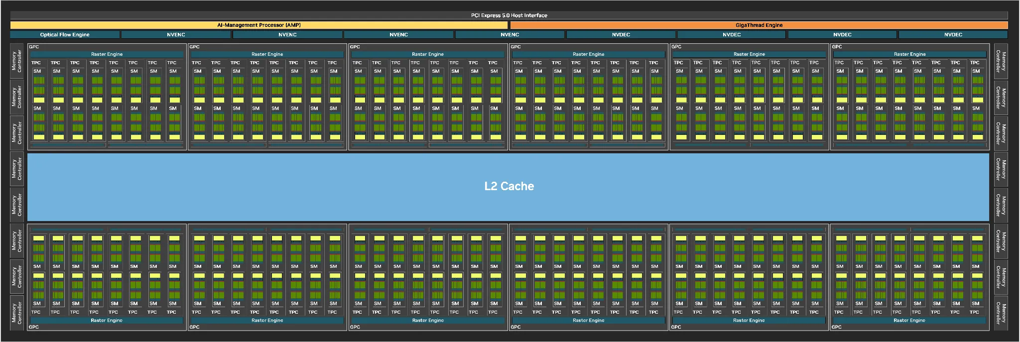
From largest to smallest, the hierarchy is:
GPU -> GPC (Graphics Processing Cluster)
    -> TPU (Texture Processing Cluster)
    -> SM  (Streaming Multiprocessor)
The core unit of a GPU is the SM. As shown below, an SM has four subpartitions, each containing:
- Control units
- Warp Scheduler: schedules assigned warps according to priority and data readiness
- Dispatch Unit: sends individual instructions to the appropriate compute units
- Compute units
- CUDA cores: execute basic scalar operations
- Tensor cores: perform multiply-accumulate (MMA) operations on two small matrices with one instruction
- SFU (Special Function Unit): handles nonlinear mathematical functions
- LD/ST: moves data to and from cache or storage
- Cache
- L0 instruction cache
- Storage
- Registers
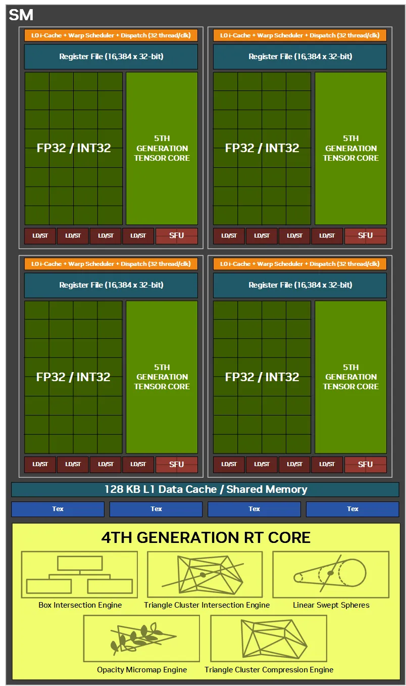
Across the entire SM, the subpartitions share:
- Share Memory
- L1 cache
- L1 Instruction Cache
- Texture Unit
The cache-related components are discussed later.
At the hardware level, this is called a SIMT architecture: Single Instruction, Multiple Threads.
In other words, one instruction controls multiple threads, or multiple threads execute the same instruction.
TODO:TMA?
2. Programming Model
CUDA core
In the programming model, the hierarchy from largest to smallest is:
Grid -> Block -> Warp -> Thread- Thread: the GPU’s basic execution unit; every thread executes the same function on different data
- Warp:
- 1 warp = 32 threads
- A warp is the smallest scheduling unit
- Threads within a warp must execute the same instruction
- Block:
- Consists of multiple threads
- Can be one-, two-, or three-dimensional
- Threads within a block share shared memory and L1 cache
- Grid:
- Consists of multiple blocks
- Different blocks in a grid cannot synchronize directly and do not share shared memory
The mapping between the hardware architecture and programming model is shown below. 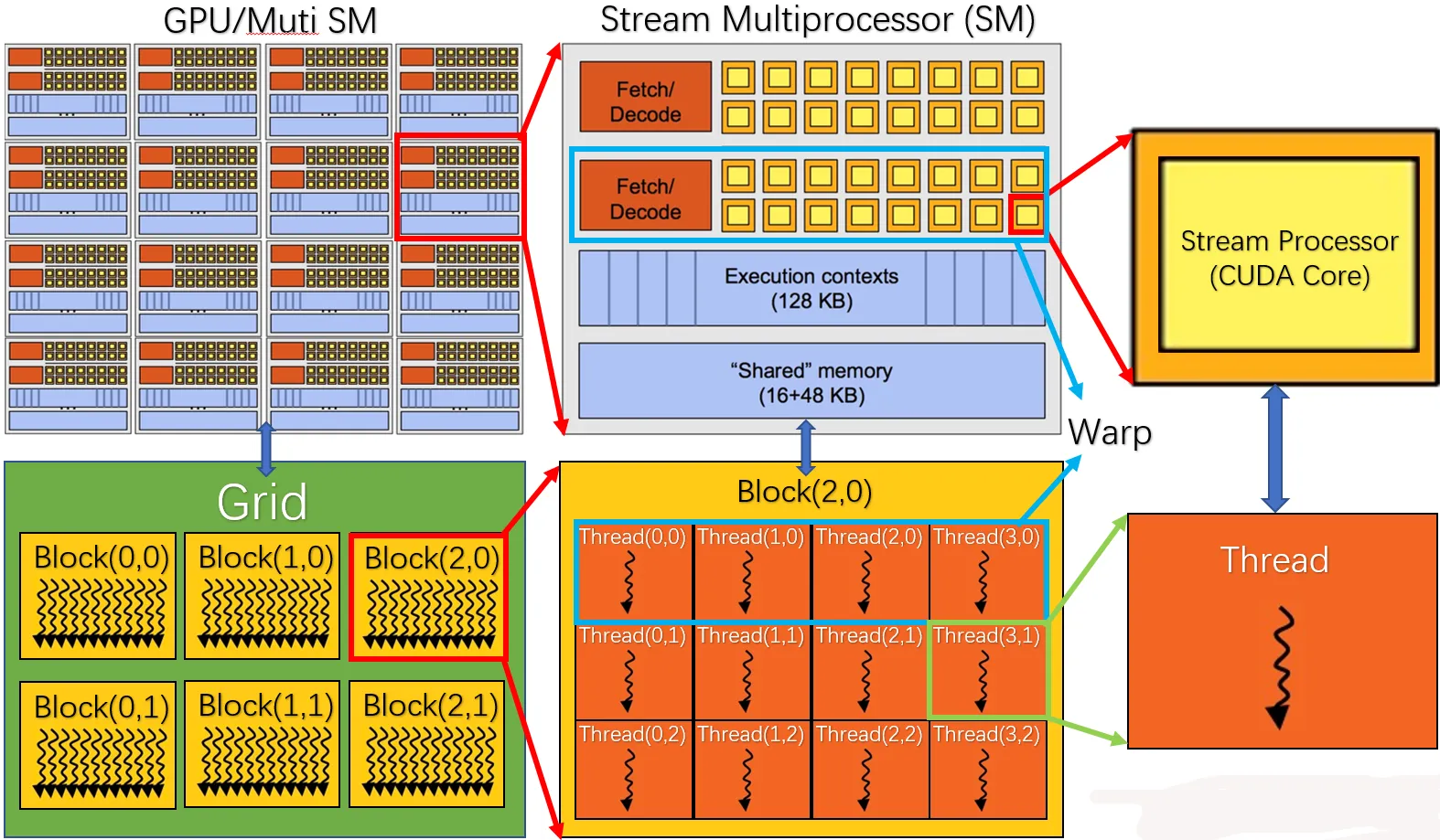
A grid is submitted to the GPU, its blocks are assigned to different SMs, the warps within each block are assigned to SM subpartitions, and individual threads are ultimately handled by CUDA cores.
To improve throughput, a single SM is often assigned multiple blocks. Resources are allocated to those blocks, and all of their warps become eligible for scheduling and execution.
The GPU follows the SIMT (Single Instruction, Multiple Threads) model. Each thread has private registers, but every thread in a warp executes the same instruction.
Consider matrix multiplication as an example of parallel programming:
// Three nested loops on the CPU
for (int i = 0; i < M; i++)
  for (int j = 0; j < N; j++)
    for (int k = 0; k < K; k++)
      C[i][j] += A[i][k] * B[k][j];
Parallel-work decomposition:
- One thread computes one element of
- One block computes one submatrix, or tile
- The whole grid covers the output matrix
Suppose a block contains threads, or eight warps. If the block is responsible for an tile, fully covering the output requires blocks in the grid.
To obtain a thread’s index—its actual coordinates in the matrix—first locate its block in the grid, then locate the thread within that block.
row = blockIdx.y * blockDim.y + threadIdx.y
col = blockIdx.x * blockDim.x + threadIdx.x
Once the indices are known, blocks are assigned to SMs and every warp executes the same code.
float sum = 0.0f;

for (int k = 0; k < K; k++) {
    sum += A[row * K + k] * B[k * N + col];
}

C[row * N + col] = sum;
This is an SPMD design: Single Program, Multiple Data.
There is only one program, but it operates on different data to complete the computation.
Tensor Core
3. Memory Design
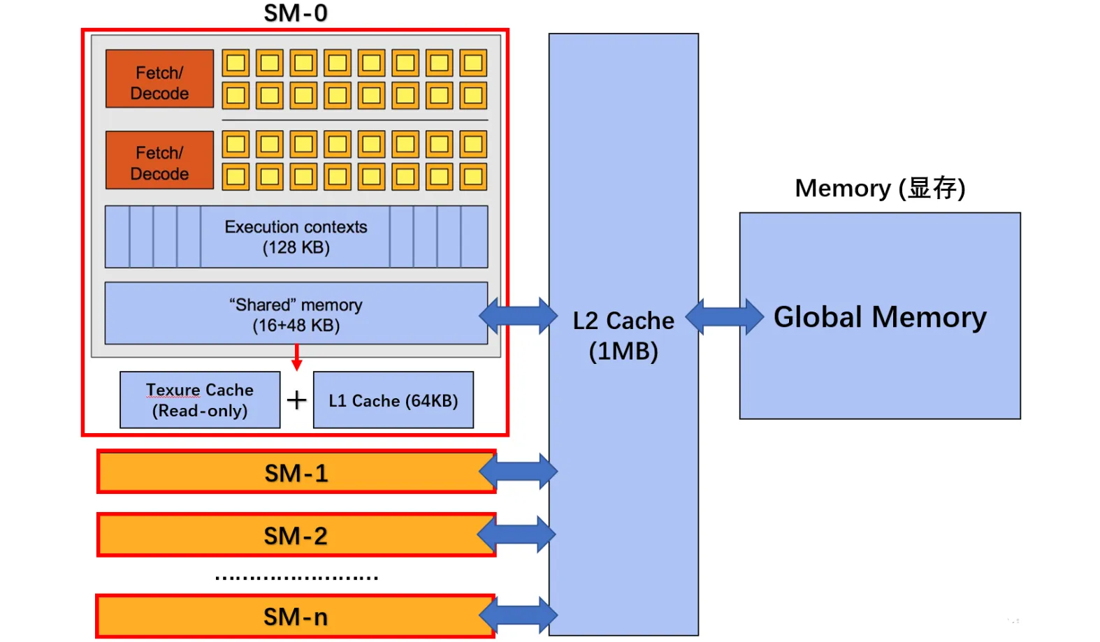
This diagram gives a clear overview of the GPU memory architecture.
Host (CPU DRAM)
        ↓ PCIe / NVLink
Global Memory (HBM / GDDR)
        ↓
L2 Cache (Chip-wide)
        ↓
Inside an SM:
    ├─ L1 Cache
    ├─ Shared Memory
    ├─ Register File
Inside an SM
Register (SRAM)
Private to each thread.
When a block is dispatched to an SM, registers are statically reserved according to compiler-determined requirements: each thread receives its own registers from the register pool.
So many physical registers are needed partly because a GPU has enormous numbers of threads. If an SM supports up to 1,024 threads and has 16,384 registers, for example, that averages 16 registers per thread.
They also enable zero-overhead switching. Unlike a CPU, the GPU maximizes throughput by keeping many warp contexts resident in registers instead of saving and restoring them through memory. In this four-subpartition example, an SM may issue instructions from up to four warps at once; registers assigned to other resident warps are temporarily idle. This still permits nearly cost-free warp rescheduling: when one warp waits for data, the scheduler selects another ready warp. Because resources were statically reserved, no new allocation is required, which improves throughput.
Shared Memory (SRAM)
- Shared by all threads in the same block
- Managed explicitly by the programmer
- Supports concurrent access
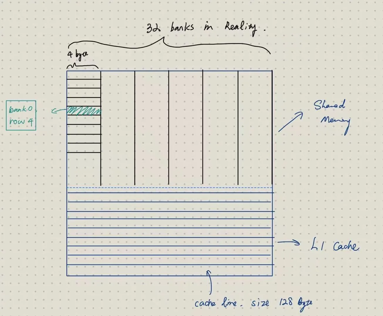
Physically, its address space is divided evenly across 32 independent banks, each with a 4-byte word width. The bank mapping determines which addresses can be accessed concurrently.
Because shared memory is allocated explicitly, it can be thought of as a programmer-managed array.
L1 Cache (SRAM)
Private to each SM and automatically caches global memory.
It shares physical SRAM capacity with shared memory.
Like a CPU cache, it is a cache-line-based store; a line is 128 bytes in this example. The cache organization and replacement policy are omitted here.
Together, the two are partitioned roughly as illustrated below; the dividing line represents a hardware-configurable boundary.
L2 Cache (SRAM)
Shared across the whole chip, reducing pressure on device-memory accesses.
Global Memory
Off-chip HBM or GDDR, with relatively high latency.
Reference
-
Some images come from this GPU architecture overview.